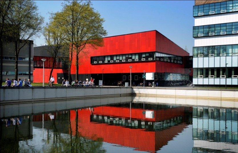
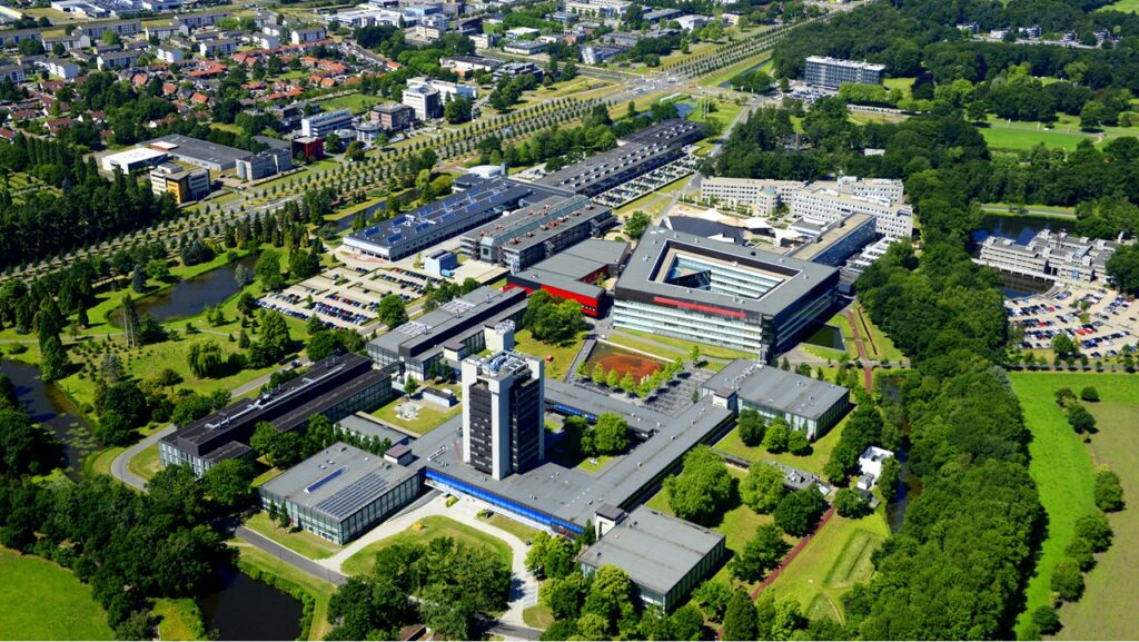
University of Twente
Description of the legal entity :
The University of Twente has around 3.300 scientists and other professionals working together on cutting- edge research, innovations with real-world relevance and inspiring education for more than 9.000 students. The enterprising university encourages students to develop an entrepreneurial spirit and is a partner of Kennispark Twente, a technology park incubator of the technologies developed at the university.
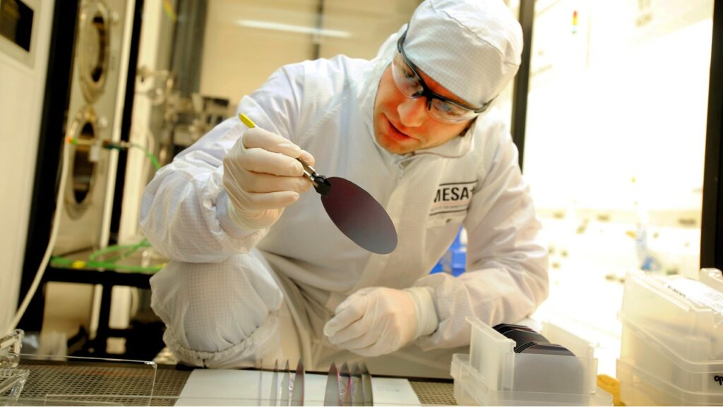
The MESA+ Institute for Nanotechnology of the University of Twente is one of the largest nanotechnology research institutes in the world, delivering competitive and high-quality research. The Institute is recognized worldwide for the high quality of its researchers. Within the MESA+ Institute for Nanotechnology, research is focused on integrated photonics, nanophotonics materials science, lab-on-a-chip technology, nanophotonics, and nanoelectronics via a multidisciplinary collaboration across groups. This method of interdisciplinary research leads to ground-breaking results, it reinforces the cohesion between ongoing high-quality research and it provides excellent opportunities for external partners.
Capitalizing on MESA+’ pioneering research activities, the UT has created a perfect habitat for start-ups in the micro and nano industry and it offers a range of educational activities such as bachelor’s and master’s degrees in Chemical Engineering, Applied Physics, Biomedical Technology, Technical Medicine, Advanced Technology and a master in Nanotechnology. The MESA+ Institute employs 525 research staff of which 275 are PhD’s or Post-Docs.
In this project, the UT will participate through the Integrated Optical Systems (IOS) group, led by prof. S.M. Garcia-Blanco. The IOS group carries out leading edge research in the field of integrated on-chip lasers and amplifiers (typically in rare-earth ion doped Al2O3, TiO2, and crystalline host materials) and integration technologies of active materials onto passive photonic platforms for different applications including optical (bio)sensing, LiDAR and metrology.
Role in the project :
The role of the UT per WP in OPHELLIA is:
The UT is leading this WP and is therefore responsible for the overall management of OPHELLIA.
UT will contribute to the analysis of end-user needs in order to translate it into the requirements of the PIC module and PIC building blocks.
The UT is leading this WP and is (jointly) responsible for:
- The development of low background loss, high gain/unit length Er3+ doped Al2O3 waveguides;
- The development of a sputtering deposition;
- The design of complex PIC modules including amplifiers, modulators and lasers.
The UT is (jointly) responsible for the development of the packaging of four laser PIC demonstrator versions.
The UT is (jointly) responsible for the exploitation and dissemination of project results.
Infrastructure and facilities :
The MESA+ Institute for Nanotechnology with 1.250 m2 of cleanroom space is fully accessible to the project team. The main nanofabrication techniques, including electron beam, nanoimprint and optical lithography, focused ion beam (FIB) etching, metal and dielectric thin film deposition, wet and dry etching, ion implantation and material characterization techniques (i.e., SEM, TEM, EDX, XPS, XR-reflectivity, ellipsometry, AFM, NSOM) are available. A reactive co-sputtering machine is available for the deposition of undoped and rare-earth (Yb3+ and Er3+) doped Al2O3 films. The available chlorine reactive ion etcher will be used for the patterning of the devices. Backend processing instruments, such as dicing and wirebonding are also available. A high positioning accuracy flip-chip bonder, the Finetech Lambda instrument, capable of controlling and ramping the T (25-400 oC), pressure (0-400 N) and atmosphere (nitrogen, air) during the bonding process, is available for integration tasks.
The IOS Lab disposes of a Logitech PM5 polishing/lapping instrument, Logitech autocollimator, ultrasonic cleaning lab and a hot-air oven. All the optical characterization equipment required for the current project are available at the IOS Labs (being a tunable Ti:Sapphire laser, an Agilent tunable laser centered at 1550 nm, various diodes and tunable laser sources, Fianium broadband source, high resolution spectrometer (Yobin-Yvon HR2000), high-resolution optical spectrum analyzers (OSA), electrical spectrum analyzers (ESA), setups for integrated optical device characterization and various optical microscopes). A commercial Metricon 2010 system is available for the characterization of the refractive index and quality of the deposited layers.
Address :
UNIVERSITY OF TWENTE
PO BOX 217
7500 AE ENSCHEDE
THE NETHERLANDS
Contact :
(+31) 53 489 9111
info@utwente.nl